Flip-flop circuits
D Flip-flop
A Latch is a basic memory device to store one bit of information. It is a sequential electronic circuit that has no CLOCK input and changes output state only in response to data input.
A Flip-flop is a clock-controlled memory device. It differs from a Latch in that it has a control signal (CLOCK) input. It stores the input state and outputs the stored state only in response to the CLOCK signal. If a Flip-flop accepts its inputs at L to H (H to L) transition, it is Positive-Edge (Negative-Edge) Triggered.
A Flip-flop is use to store one bit of information. By connecting several Flip-flops together, they may store data that can represent the state of a sequencer, the value of a counter, an ASCII character in a computer's memory or any other piece of information.
D Flip-flop is one of the most commonly used Flip-flops. For a Positive-Edge-Triggered D Flip-flop, its output Q follows input D only at every L to H transition of CLOCK, otherwise, Q keeps unchanged. Figure 1 shows the Timing Diagram of a Positive-Edge-Triggered D Flip-flop and Table 1 is its Truth-Table.
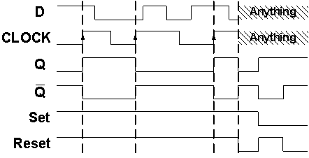
Figure 1: Timing Diagram of a Positive-Edge-Triggered D Flip-flop
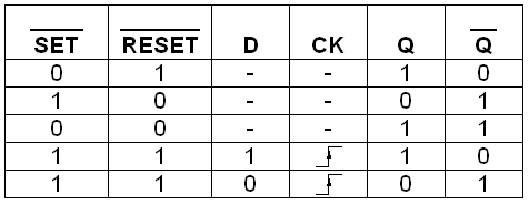
Table 1: D Flip-flop Truth-Table
SET and RESET are two additional inputs to override the clocked operation of the D Flip-flop. For the D Flip-flop to operate, both SET and RESET must be 1.
The first electronic Flip-flop was invented in 1919. Four types of Flip-flops are common used in clocked sequential systems: they are called the T Flip-flop, the S-R Flip-flop, the J-K Flip-flop, and the D Flip-flop.
J-K Flip-flop Binary Counter
A Counter is a device, which stores (and sometimes displays) the number of times a particular event has occurred, often in relationship to a CLOCK Signal. In electronics, counters can be implemented quite easily using memory devices such as Flip-flops.
J-K Flip-flop is one of the most commonly used Flip-flops. Table 1 is the Truth-Table of a Negative-Edge-Triggered J-K Flip-flop.
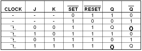
Table 2: J-K Flip-flop Truth-Table
In Figure 2, four Negative-Edge-Triggered J-K Flip-flops are connected in a cascade mode (the output Q of one Flip-flop is connected to the input CLOCK of the next Flip-flop) to form a Binary Counter. Inputs J and K of each Flip-flop are always 1, according to the Truth-Table, the Flip-flop changes its state upon each H to L transition of its CLOCK.
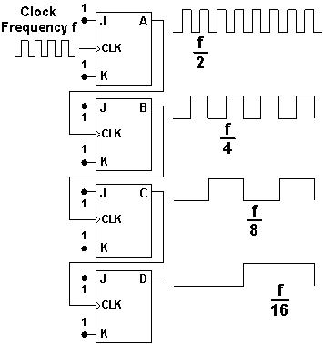
Figure 1: Timing Diagram of the J-K Flip-flop Counter
In this Binary Counter, outputs A to D represent a 4-bit Binary Number, in which A is the LSB and D is the MSB.
The 4-bit Binary Number is increased by one on each CLOCK cycle. The count goes from (0)10 to (15)10 and then cycles back to (0)10, Table 3.
| Decimal | Binary | |||
|---|---|---|---|---|
| D | C | B | A | |
| 0 | 0 | 0 | 0 | 0 |
| 1 | 0 | 0 | 0 | 1 |
| 2 | 0 | 0 | 1 | 0 |
| 3 | 0 | 0 | 1 | 1 |
| 4 | 0 | 1 | 0 | 0 |
| 5 | 0 | 1 | 0 | 1 |
| 6 | 0 | 1 | 1 | 0 |
| 7 | 0 | 1 | 1 | 1 |
| 8 | 1 | 0 | 0 | 0 |
| 9 | 1 | 0 | 0 | 1 |
| 10 | 1 | 0 | 1 | 0 |
| 11 | 1 | 0 | 1 | 1 |
| 12 | 1 | 1 | 0 | 0 |
| 13 | 1 | 1 | 0 | 1 |
| 14 | 1 | 1 | 1 | 0 |
| 15 | 1 | 1 | 1 | 1 |
Table 3: Truth-Table of a 4-bit Binary Counter
8 Bit Shift Register
A Register is a device for storing data in Digital Circuits. The Register is a collection of two or more Flip-flops with a common CLOCK input. Registers are often used to store a collection of related bits, such as a byte of data in a computer.
A Shift Register is a Multi-bit Register, which shifts its stored data by one bit position at each CLOCK transition. In the Shift Register, a group of Flip-flops are linked up such that the output of a Flip-flop is connected to the input of the next. As a result, data is shifted down the line when the CLOCK is activated.
For a 8 Bit Shift Register, at every CLOCK transition from L to H, the Shift Register reads input DATA and transfers it to output A0. Each previous value of bit A0 to A6 is shifted to the next bit (that is, A0 to A1, A1 to A2, … , A6 to A7), and the value of A7 is shifted out of the register. Table 4 illustrates this operation.
| A0 | A1 | A2 | A3 | A4 | A5 | A6 | A7 | |
|---|---|---|---|---|---|---|---|---|
| Initial States | 0 | 0 | 0 | 0 | 0 | 0 | 0 | 0 |
| Clock cycle 1 | 1 | 0 | 0 | 0 | 0 | 0 | 0 | 0 |
| Clock cycle 2 | 0 | 1 | 0 | 0 | 0 | 0 | 0 | 0 |
| Clock cycle 3 | 0 | 0 | 1 | 0 | 0 | 0 | 0 | 0 |
| Clock cycle 4 | 0 | 0 | 0 | 1 | 0 | 0 | 0 | 0 |
| Clock cycle 5 | 0 | 0 | 0 | 0 | 1 | 0 | 0 | 0 |
| Clock cycle 6 | 0 | 0 | 0 | 0 | 0 | 1 | 0 | 0 |
| Clock cycle 7 | 0 | 0 | 0 | 0 | 0 | 0 | 1 | 0 |
| Clock cycle 8 | 0 | 0 | 0 | 0 | 0 | 0 | 0 | 1 |
Table 4: Shifting process of the Shift Register in 8 clock cycles
Shift registers can have a combination of serial and parallel inputs and outputs. Serial-in means the device reads in the data bit by bit, and Parallel-out means all the output bits are presented simultaneously. For example a serial-in, parallel-out Shift Register is one that reads in the data bit by bit, and presents the output bits simultaneously.
One of the most common uses of a Shift Register is to convert between serial and parallel interfaces. This is useful, as many circuits work on groups of bits in parallel, but serial interfaces are simpler to construct.
A Shift Register can be used as a simple delay circuit. At different outputs (A0 to A7), DATA is delayed by different clock cycles.
About CMM
Contact US
Others
Other Websites
Number of Visitors:
Last Modified Date: 10/3/2025