How an npn Bipolar Junction Transistor (BJT) works
Bipolar Junction Transistor (BJT) is a Semiconductor device constructed with three doped Semiconductor Regions (Base, Collector and Emitter) separated by two p-n Junctions, Figure 1. The p-n Junction between the Base and the Emitter has a Barrier Voltage (V0) of about 0.6 V, which is an important parameter of a BJT. Unlike the Field Effect Transistor (FET), in which Current is produced only by one type of Charge Carrier (Electrons or Holes), in BJT, Current is produced by both types of Charge Carriers (Electrons and Holes), hence the name Bipolar.
 Figure 1: Bipolar Junction Transistor
There are two Types of BJT: npn and pnp. The npn Type consists of two n-Regions separated by a p-Region. The pnp Type consists of two p-Regions separated by an n-Region. Figures 2 and Figure 3 are their schematic symbols respectively. The following explanation focuses on the npn BJT.
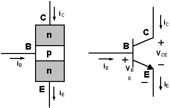 Figure 2: Schematic symbol of an npn, BJT
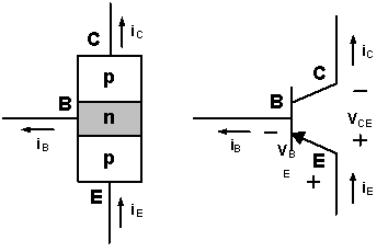 Figure 3: Schematic symbol of a pnp, BJT
The BJT operates in three different modes: Cutoff mode, Linear Amplification mode and Saturation mode, Figure 4. Table 1 is a summary of the three Operation Modes of an npn BJT.
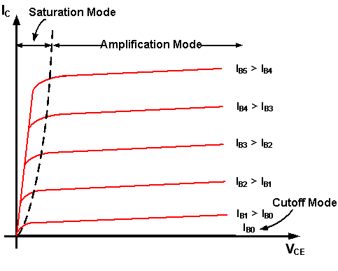 Figure 4: IC-VCE Characteristics Curves of an npn BJT
BJT is very important in electronics. They are used extensively in other Exhibits, especially as Amplifiers in analog circuit and Electronic Switches in digital circuit.
About CMM
Contact US
Others
Other Websites
Number of Visitors:
Last Modified Date: 10/3/2025